


PiBond pioneers a new material approach for MEMS and 3D IC manufacturing.
/INS. PiBond today announced the latest key milestone in its innovative SAP platform. SAP’s metal oxide solution revolutionizes the way in which manufacturers deal with ever increasing cost structures resulting from more complex designs. These materials boast higher etch selectivity than anything currently on the market - thus enabling patterning architectures previously unavailable with conventional techniques.
“The SAP platform is a breakthrough in the way manufacturers can deal with ever growing challenges faced by the semiconductor industry,” said Jonathan Glen, Chairman and Managing Director of Pibond. “It is a simple solution to the current road block that is holding back the development of a new generations of devices demanded by the market.”
The material developed by PiBond has the ability to withstand variable aggressive reactive ion etch conditions. The patent granted materials boast etch selectivity to silicon that exceeds 100 000:1 - improving the control of critical dimensions, and enabling patterning architectures previously unachievable with conventional techniques. The SAP products are easy-to-apply and easy-to-remove spin coated materials which can be processed using existing coating infrastructure.
As well as working as normal hard-masks, SAP’s photo-patterned metal oxide materials are expected to revolutionize pattern and etch cost structures by the elimination of cumbersome thick photoresists as well as costly and slow plasma vapor deposition tools. With a photo-patterned SAP product PiBond anticipates to reduce costs considerably. “We believe this material platform will fundamentally change how our users approach patterning these demanding architectures” adds Dr. Thomas Gädda, Director at PiBond.
SAP products are anticipated to become the go-to material not only in the MEMS industry but also in DRAM memory capacitor trench generations and 3D IC through silicon via (TSV) patterning and in particular the System-on-Package Backside Illuminated CMOS image sensor.
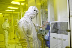
Caption: Pibond is awarded patent for its SAP technology platform. © Pibond
About PiBond
PiBond is a leader in the development and production of advanced liquid spin-on materials based on organosilicon and metal-oxide chemistries. PiBond has a proven track record of materials innovation and manufacturing for the semiconductor industry. The company (formally known as Silecs) continues to serve existing and new customers with products meeting the industry’s stringent quality requirements. PiBond’s technology and state-of-the-art production facility in Finland, and products are key contributors in the production of the latest ultra-high resolution semiconductor devices used in mobile, electric vehicles and wearable devices. A global provider with a proven and audited track-record of producing and monitoring specialty chemicals at ultra-high purity levels where impurities are within the parts-per-trillion level.
Contact:
PiBond Oy
Kutojantie 2 B 02630 Espoo, Finland
info@pibond.com – www.pibond.com


Let us know if you are going to use this press release. Thank you!