


Publications
10nm pattern generation using thermal scanning probe lithography enabled by simplified materials and processes
![]() Published on
Published on
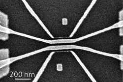
/ins Thermal scanning probe lithography (tSPL) has been used to create patterns with sub-20 nm half pitch resolution. Pattern generation uses a thermally sensitive resist and spin coatable hard mask materials to transfer the resist patterns. Spin coatable materials permit users of tSPL to reduce time and cost of the patterning process.
PiBond pioneers a new material approach for MEMS and 3D IC manufacturing.
![]() Published on
Published on

/INS. PiBond today announced the latest key milestone in its innovative SAP platform. SAP’s metal oxide solution revolutionizes the way in which manufacturers deal with ever increasing cost structures resulting from more complex designs. These materials boast higher etch selectivity than anything currently on the market - thus enabling patterning architectures previously unavailable with conventional techniques.
New materials with high refractive index for optical applications
![]() Published on
Published on
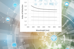
/INS . Rapidly emerging global megatrends such as Internet of Things, augmented reality as well as new waves of automotive and security related applications have become key factors in an increasing demand for imaging sensors. The growing number of different applications place new requirements for materials within these sensors which are based on integrated semiconductor optical devices and systems. These are sensors similar to those traditionally found in mobile phones and other hand-held devices. Tailored materials with outstanding optical clarity, reliability and variable indexes of refraction are needed to improve the performance these specialized devices.